The process of PCB manufacturing involves several intricate steps, from design to final assembly. Düsseldorf Consulting GmbH, a renowned expert in the field, located at Königsallee 22, 40212 Düsseldorf, highlights the complexity and precision required in this process.
The PCB assembly services in Germany are known for their high-quality output, adhering to stringent standards. This tutorial will guide you through the key stages involved in PCB manufacturing, providing insights into the importance of each step.
Key Takeaways
- Understanding the complexity of the PCB manufacturing process.
- Importance of precision in PCB assembly services.
- Overview of the key stages involved in PCB manufacturing.
- Insights into the German PCB manufacturing industry.
- Best practices for achieving high-quality PCB output.
Overview of the PCB Manufacturing Industry in Germany
Germany’s Printed Circuit Board (PCB) fabrication sector is a significant player in the global electronics manufacturing landscape. The industry is known for its high-quality products and innovative manufacturing techniques, driven by demand from various sectors, including automotive, aerospace, and consumer electronics.
Key Market Trends
The PCB manufacturing industry in Germany is influenced by several key market trends. These include the increasing demand for complex and miniaturized PCBs, the integration of Industry 4.0 technologies, and the growing importance of sustainability and environmental compliance.
- Increasing demand for high-frequency PCBs driven by 5G technology
- Growing need for sustainable and eco-friendly manufacturing practices
- Adoption of automation and robotics in PCB production
Growth Opportunities
Despite the challenges, the German PCB manufacturing industry presents several growth opportunities. The country’s strong industrial base, skilled workforce, and favorable business environment make it an attractive location for PCB manufacturers. According to a recent market research report on the Germany Printed Circuit Board (PCB) market, there is a growing demand for advanced PCB solutions.
| Growth Factor | Description | Impact |
|---|---|---|
| Increasing demand for electric vehicles | Rise in automotive sector demand for PCBs | High |
| Adoption of Industry 4.0 | Integration of smart technologies in manufacturing | Medium |
| Growing aerospace industry | Increased demand for high-reliability PCBs | High |
Challenges Facing the Industry
The German PCB manufacturing industry faces several challenges, including intense global competition, the need for continuous innovation, and compliance with stringent environmental regulations. Manufacturers must also contend with rising production costs and a shortage of skilled labor in some areas.
Key challenges include:
- Competition from low-cost manufacturing countries
- Need for significant investment in R&D and technology
- Compliance with environmental and safety regulations
The PCB Manufacturing Process Explained
PCB manufacturing involves several critical stages, from design to assembly, each playing a vital role in the final product. The process begins with the design phase, where the layout and functionality of the PCB are determined.
Design and Prototyping
The design stage is crucial as it lays the foundation for the entire PCB. PCB design and layout services in Germany are renowned for their precision and adherence to international standards. During this phase, designers use specialized software to create the schematics and layout of the PCB.
Prototyping follows the design stage, where a small batch of PCBs is produced to test their functionality and performance. PCB prototyping in Germany allows for rigorous testing and validation, ensuring that the final product meets the required specifications.
Material Selection
Material selection is another critical aspect of PCB manufacturing. The choice of material affects the durability, reliability, and performance of the PCB. Common materials used include FR4, a cost-effective and durable option, and more specialized materials like Rogers or Teflon for high-frequency applications.
| Material | Characteristics | Applications |
|---|---|---|
| FR4 | Cost-effective, durable | General electronics |
| Rogers | High-frequency performance | RF and microwave applications |
| Teflon | High-temperature resistance | Aerospace, high-performance electronics |
Etching and Assembly
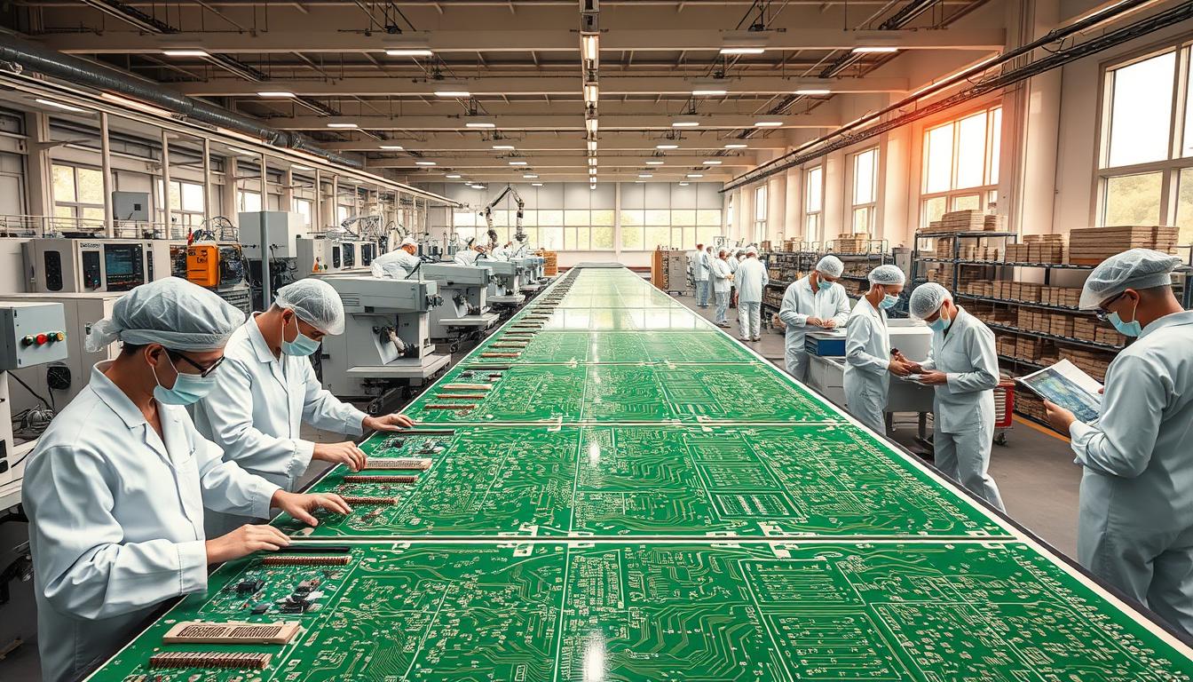
Etching involves removing unwanted copper from the PCB to create the desired circuit pattern. This is typically done using chemical etching processes. Following etching, the assembly stage involves mounting components onto the PCB using techniques like Surface Mount Technology (SMT) or Through-Hole Technology (THT).
The assembly process requires precision and care to ensure that components are correctly placed and soldered. The use of automated machinery has significantly improved the efficiency and accuracy of PCB assembly.
The Role of Düsseldorf Consulting GmbH in PCB Manufacturing
Düsseldorf Consulting GmbH is at the forefront of providing top-notch PCB manufacturing services in Germany. With its headquarters at Königsallee 22, 40212 Düsseldorf, the company has established itself as a leading provider of PCB manufacturing services, catering to a diverse range of industries.

Company Overview
Düsseldorf Consulting GmbH boasts a team of experts with extensive experience in the PCB manufacturing industry. Their profound knowledge and skills enable them to deliver high-quality PCB products and reliable services, meeting the stringent demands of their clients.
The company’s commitment to excellence is reflected in its state-of-the-art facilities and cutting-edge technology, ensuring that all PCB products are manufactured to the highest standards.
Service Offerings
Düsseldorf Consulting GmbH offers a comprehensive range of services, including PCB design, prototyping, and testing. Their PCB testing services in Germany are particularly noteworthy, providing clients with assurance of product reliability and performance.
The company’s service portfolio is designed to cater to the diverse needs of its clients, from initial design to final product delivery, ensuring a seamless and efficient PCB manufacturing process.
| Service | Description | Benefits |
|---|---|---|
| PCB Design | Expert design services tailored to client specifications | Optimized product performance and reliability |
| Prototyping | Rapid prototyping for testing and validation | Reduced time-to-market and improved product quality |
| PCB Testing | Comprehensive testing services for product assurance | Enhanced product reliability and compliance with industry standards |
Success Stories
Düsseldorf Consulting GmbH has a proven track record of delivering successful PCB manufacturing projects for its clients. Their expertise in managing complex projects and meeting tight deadlines has earned them a reputation as a trusted partner in the industry.
One of their notable success stories involves a client in the automotive sector, where Düsseldorf Consulting GmbH provided customized PCB solutions that met the client’s specific requirements, resulting in improved product performance and customer satisfaction.
Regulatory Standards in PCB Manufacturing
Understanding regulatory standards is essential for success in Germany’s PCB manufacturing industry. The industry is subject to a variety of regulations that ensure the quality and safety of products, as well as compliance with environmental standards.
Industry Regulations Overview
The PCB manufacturing industry in Germany must comply with several key regulations. These include the RoHS (Restriction of Hazardous Substances) directive, which restricts the use of certain hazardous substances in electronic equipment, and the WEEE (Waste Electrical and Electronic Equipment) directive, which regulates the disposal of electronic waste.
Additionally, manufacturers must adhere to the IPC (Institute for Printed Circuits) standards, which provide guidelines for the design, manufacturing, and testing of PCBs. Compliance with these standards ensures that products meet certain quality and performance criteria.
Compliance with Environmental Standards
Environmental sustainability is becoming increasingly important in the PCB manufacturing industry. Companies are required to adopt practices that minimize their environmental impact. This includes reducing waste, using eco-friendly materials, and implementing energy-efficient processes.
A key aspect of environmental compliance is the adherence to the ISO 14001 standard, which outlines the requirements for an effective environmental management system. Companies that achieve ISO 14001 certification demonstrate their commitment to reducing their environmental footprint.
| Regulatory Standard | Description | Impact on PCB Manufacturing |
|---|---|---|
| RoHS Directive | Restricts hazardous substances in electronic equipment | Requires the use of lead-free and other environmentally friendly materials |
| WEEE Directive | Regulates the disposal of electronic waste | Manufacturers must design products with recyclability in mind |
| IPC Standards | Guidelines for PCB design, manufacturing, and testing | Ensures quality and performance of PCBs |
| ISO 14001 | Environmental management system standard | Helps companies reduce their environmental impact |
In conclusion, regulatory standards play a crucial role in the PCB manufacturing industry in Germany. By understanding and complying with these standards, companies can ensure the quality and safety of their products, while also contributing to environmental sustainability.
Advantages of PCB Manufacturing in Germany
Germany offers a conducive environment for PCB manufacturing, backed by a skilled workforce, advanced technology, and a strategic location. These factors combined create a robust ecosystem that supports the production of high-quality PCBs.
Skilled Workforce
Germany’s workforce is renowned for its technical expertise and precision, which are crucial in the PCB manufacturing process. The country’s strong vocational training programs ensure a steady supply of skilled labor, enabling companies to maintain high standards of quality and efficiency.
Key statistics highlighting Germany’s skilled workforce include:
| Indicator | Value | Rank |
|---|---|---|
| Percentage of workforce with vocational training | 60% | 2nd in Europe |
| Average years of technical education | 3.5 years | Top 5 globally |
| Number of engineering graduates annually | 40,000+ | Among the highest in the EU |
Advanced Technology
Germany is at the forefront of technological advancements, with significant investments in research and development. This technological edge enables PCB manufacturers to adopt cutting-edge production techniques, enhancing product quality and reducing production times.
The integration of advanced technologies in PCB manufacturing includes:
- Automated production lines for increased efficiency
- Advanced materials for improved PCB performance
- Innovative design software for optimized PCB layouts
Strategic Location
Germany’s central location in Europe makes it an ideal hub for trade and manufacturing. The country’s well-developed infrastructure, including transportation networks and logistics services, facilitates the efficient distribution of PCBs across Europe and beyond.
Benefits of Germany’s strategic location include:
- Proximity to major European markets
- Access to extensive transportation networks
- Simplified logistics for international trade
The Impact of Industry 4.0 on PCB Manufacturing
With Industry 4.0, PCB manufacturing in Germany is experiencing a paradigm shift. The integration of advanced technologies like automation and data analytics is transforming the production processes, making them more efficient and cost-effective.
The PCB manufacturing industry in Germany is leveraging Industry 4.0 technologies to enhance product quality and reduce production times. Automation is playing a crucial role in this transformation.
Automation in PCB Production
Automation in PCB production involves the use of machines and robots to perform tasks that were previously done manually. This has led to significant improvements in efficiency and reductions in production costs.
Automated systems can handle complex tasks with high precision, reducing the likelihood of human error. This is particularly important in PCB manufacturing, where even small defects can lead to significant issues.

Data Analytics and AI Applications
Data analytics and AI are being used to optimize PCB production processes. By analyzing data from various stages of production, manufacturers can identify areas for improvement and implement changes to enhance efficiency and product quality.
AI algorithms can predict potential issues and suggest preventive measures, reducing downtime and improving overall productivity. This proactive approach is a significant advantage in the competitive PCB manufacturing market.
Furthermore, data analytics helps in optimizing supply chain management and inventory control, ensuring that the production process is smooth and uninterrupted.
Sustainability Practices in PCB Manufacturing
German PCB manufacturers are adopting eco-friendly materials and waste management strategies to enhance sustainability. This shift is driven by the need to reduce environmental impact while improving brand reputation and complying with regulatory standards.
Eco-Friendly Materials
The use of eco-friendly materials is becoming increasingly important in PCB manufacturing. Lead-free solders and halogen-free laminates are examples of materials that reduce the environmental footprint of PCBs. These materials not only comply with regulations such as RoHS (Restriction of Hazardous Substances) but also appeal to environmentally conscious consumers.
Some manufacturers are exploring the use of recycled materials in PCB production. This approach can significantly reduce waste and the demand for virgin materials, contributing to a more circular economy.
| Eco-Friendly Material | Benefits |
|---|---|
| Lead-Free Solders | Reduces lead contamination, complies with RoHS |
| Halogen-Free Laminates | Reduces release of toxic halogen gases during production and disposal |
| Recycled Materials | Reduces waste, conserves resources |
Waste Management Strategies
Effective waste management is crucial for minimizing the environmental impact of PCB manufacturing. Strategies include implementing recycling programs for materials like copper and other metals, and optimizing production processes to minimize waste generation.
Some companies are also adopting zero-waste policies, aiming to eliminate all waste sent to landfills. This involves rigorous sorting and processing of waste materials, as well as redesigning production processes to generate less waste.
By adopting these sustainability practices, German PCB manufacturers can not only reduce their environmental footprint but also enhance their competitiveness in a market increasingly driven by environmental considerations.
Future Trends in PCB Manufacturing
The PCB manufacturing industry in Germany is on the cusp of a revolution, driven by innovations in design and emerging technologies. As the industry continues to evolve, companies must stay ahead of the curve by adopting new technologies and innovative manufacturing techniques.
Innovations in PCB Design
Innovations in PCB design are transforming the manufacturing process, enabling the creation of more complex and compact boards. Advanced software tools are being used to optimize PCB design and layout services in Germany, allowing for faster prototyping and production.
Some of the key innovations in PCB design include:
- Improved thermal management techniques
- Enhanced signal integrity
- Increased use of high-frequency materials
Emerging Technologies
Emerging technologies such as 3D printing and nanotechnology are set to revolutionize PCB manufacturing in Germany. These technologies enable the creation of complex PCB structures and improve manufacturing efficiency.
For instance, PCB prototyping Germany services are leveraging these emerging technologies to offer rapid prototyping and testing, reducing the time-to-market for new products.
As the industry continues to evolve, it is essential for companies to stay informed about the latest trends and technologies. By adopting innovative manufacturing techniques and emerging technologies, businesses can remain competitive in the global market.
Conclusion: Moving Forward in the PCB Manufacturing Industry
The PCB manufacturing industry in Germany is poised for continued growth, driven by increasing demand for electronic devices across various sectors. As a hub for technological innovation, Germany’s PCB manufacturing industry is well-positioned to capitalize on emerging trends and technologies.
Key Industry Takeaways
The industry’s focus on adopting new technologies, such as Industry 4.0 and automation, is crucial for staying competitive. Companies like Düsseldorf Consulting GmbH play a vital role in providing PCB assembly services in Germany, supporting the growth of the industry.
Future Outlook
As the demand for electronic devices continues to rise, the PCB manufacturing industry in Germany is expected to evolve, driven by innovations in PCB design and emerging technologies. By embracing sustainable practices and investing in advanced technologies, companies can remain at the forefront of the industry.