The photolithography and microfabrication sector is a significant contributor to Germany’s technological advancements. Düsseldorf Consulting GmbH, located at Königsallee 22, 40212 Düsseldorf, is a key player in this industry, providing expert consulting services.
The Germany Direct-write Photolithography Systems Market is experiencing substantial growth, with a valuation of USD 0.1 Billion in 2024. It is projected to reach USD 0.3 Billion by 2033, indicating a promising future for this sector.
This growth is driven by the increasing demand for advanced microfabrication techniques. As a result, the sector is expected to witness significant developments in the coming years.
Key Takeaways
- The Germany Direct-write Photolithography Systems Market is projected to reach USD 0.3 Billion by 2033.
- Düsseldorf Consulting GmbH is a key player in the photolithography and microfabrication sector.
- The sector is driven by the increasing demand for advanced microfabrication techniques.
- Significant growth is expected in the coming years.
- The market size was valued at USD 0.1 Billion in 2024.
Introduction to Photolithography and Microfabrication
At the heart of semiconductor manufacturing and beyond, photolithography and microfabrication play crucial roles. These technologies are fundamental to producing the tiny components that power modern electronics.
What is Photolithography?
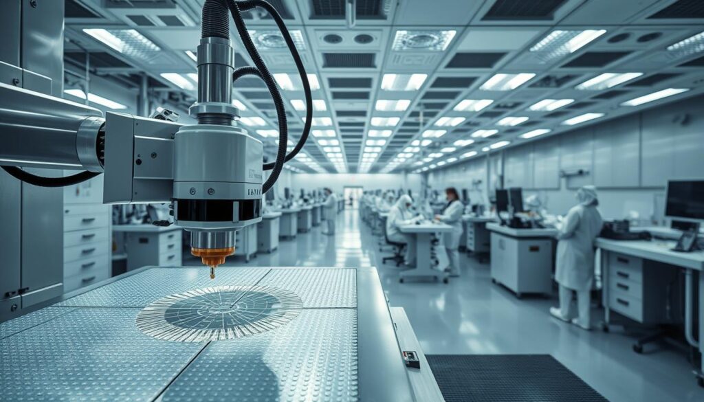
Photolithography is a process used to create the microscopic patterns on semiconductor materials, which are essential for the production of microelectronic devices. It involves the transfer of patterns onto a substrate using light, allowing for the precise creation of complex structures. Companies like Heidelberg Instruments have been at the forefront of enhancing lithography systems, achieving significant advancements such as a 200 nm resolution in their DWL66+ system.
Importance in Modern Manufacturing
The importance of photolithography in modern manufacturing cannot be overstated. It is a critical step in the production of semiconductors, which are used in a wide range of applications, from consumer electronics to automotive and medical devices. The precision and accuracy provided by photolithography enable the production of smaller, faster, and more efficient electronic components.
Overview of Microfabrication Techniques
Microfabrication encompasses a variety of techniques used to fabricate miniature structures on a microscopic scale. These techniques include photolithography, etching, and doping, among others. Microfabrication is not limited to semiconductor manufacturing; it is also used in the production of medical devices, sensors, and other microelectromechanical systems (MEMS). The advancements in microfabrication techniques have been driven by the demand for smaller, more complex devices, and lithography equipment suppliers have played a vital role in this progress.
The Evolution of the Photolithography Sector
With a strong foundation in research and development, Germany’s photolithography sector has continued to innovate, pushing the boundaries of what is possible in microfabrication. Berlin, being a hub for research institutions and universities, has significantly contributed to the advancement of photolithography techniques.
Historical Context in Germany
Germany’s photolithography sector has a rich history that dates back several decades. The country’s strong emphasis on engineering and manufacturing laid the groundwork for the development of sophisticated photolithography technologies.
The historical context is marked by significant investments in research and development, which have enabled the sector to evolve and adapt to changing technological landscapes. Key research institutions and universities have played a crucial role in driving innovation.
Key Milestones and Innovations
Several key milestones have defined the evolution of the photolithography sector in Germany. Some of the notable innovations include:
- The development of advanced lithography techniques, such as nanoimprint lithography, which have enabled the creation of smaller, more complex microelectronic components.
- Improvements in resolution and accuracy, allowing for more precise manufacturing processes.
- The integration of new materials and technologies, further enhancing the capabilities of photolithography.
Current Trends Driving Growth
The photolithography sector in Germany is currently driven by several trends, including the increasing demand for microelectronic components in various industries. The development of nanoimprint lithography is a significant trend, offering high-resolution patterning capabilities at lower costs.
Other trends include the adoption of advanced manufacturing technologies and the growing importance of sustainability in production processes. As the sector continues to evolve, it is likely that new innovations will emerge, further driving growth and development.
The future of photolithography in Germany looks promising, with ongoing research and development expected to yield new breakthroughs and applications. The sector’s ability to adapt to changing technological and market demands will be crucial to its continued success.
Major Companies in Germany’s Microfabrication Landscape
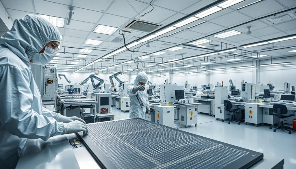
Germany’s microfabrication industry is characterized by a strong presence of companies specializing in cleanroom facilities and mask aligners. These companies are crucial for the advancement of microfabrication technologies.
Düsseldorf Consulting GmbH Overview
Düsseldorf Consulting GmbH, located at Königsallee 22, 40212 Düsseldorf, plays a significant role in the microfabrication sector. The company provides consulting services that cater to the specific needs of the industry, including guidance on cleanroom facilities and microfabrication techniques.
Other Key Industry Players
Several other companies are prominent in Germany’s microfabrication landscape. These include:
- Nanoscribe, known for their innovative 3D printing technology.
- Heidelberg Instruments, a leading manufacturer of mask aligners and other lithography systems.
- Raith, specializing in electron beam lithography and other nanofabrication tools.
- KLOE, a company that provides lithography and etching solutions.
- Durham Magneto Optics, contributing to advancements in magneto-optical technologies.
- SVG Optronics, involved in the development of optronic systems.
These companies, along with Düsseldorf Consulting GmbH, form a robust ecosystem that drives innovation in microfabrication.
Collaboration and Partnerships
The microfabrication industry in Germany thrives on collaboration and partnerships among companies, research institutions, and government bodies. Such collaborations facilitate the sharing of knowledge, resources, and risk, leading to accelerated innovation and growth. For instance, partnerships between mask aligners manufacturers and research institutions have led to significant advancements in lithography technologies.
The importance of cleanroom facilities cannot be overstated, as they provide the controlled environments necessary for the production of microfabricated devices. Companies that specialize in designing and equipping these facilities play a critical role in supporting the industry’s infrastructure.
Applications of Photolithography in Various Industries
With its precision and versatility, photolithography is instrumental in the development and production of cutting-edge technologies across multiple industries. This technology enables the creation of micro-scale patterns on surfaces, a critical process in the fabrication of modern electronic and medical devices.

Semiconductor Manufacturing
In the semiconductor industry, photolithography is a cornerstone technology used to create the intricate patterns on silicon wafers that become integrated circuits. The process involves the use of photomasks, which are essentially templates that define the pattern to be transferred onto the semiconductor material. The precision offered by photolithography is crucial for the production of smaller, faster, and more efficient chips.
The role of photomask production is particularly significant as it directly affects the quality and complexity of the semiconductor devices. Advanced photomask technologies enable the fabrication of chips with higher transistor densities, contributing to the ongoing miniaturization of electronic devices.
Medical Devices and Biotech
Photolithography also finds extensive applications in the medical devices and biotechnology sectors. It is used to fabricate components for diagnostic equipment, implants, and other medical devices that require high precision. For instance, lab-on-a-chip devices, which are used for various diagnostic tests, rely on photolithographic techniques for their manufacture.
In biotech, photolithography is utilized in the development of microarrays for genetic analysis and other applications that require the precise patterning of biological molecules on surfaces.
Consumer Electronics Production
The consumer electronics industry benefits significantly from photolithography, particularly in the production of displays, sensors, and other components that require microfabrication. The technology enables the creation of high-resolution displays and compact sensors that are integral to modern smartphones, tablets, and other consumer electronics.
Moreover, the advancements in photomask technology have facilitated the development of more sophisticated consumer electronics, with features such as higher screen resolutions and more compact designs.
Regional Hubs of Microfabrication in Germany
Regional hubs across Germany play a crucial role in the development of microfabrication technologies. These hubs are not only centers of innovation but also foster collaboration among industry players, research institutions, and government bodies.
Düsseldorf: The Heart of Innovation
Düsseldorf is recognized as a significant hub for the microelectronics industry in Germany. Companies like Düsseldorf Consulting GmbH are pivotal in driving innovation and providing specialized services to the microfabrication sector.
The city’s strategic location and well-developed infrastructure make it an attractive location for businesses and research institutions alike.
Other Notable Cities
Besides Düsseldorf, other cities in Germany are making significant contributions to the microfabrication landscape. Berlin, for instance, is known for its vibrant startup scene and research institutions that are advancing microelectronics.
Other notable cities include Munich, Stuttgart, and Dresden, each with its unique strengths and contributions to the industry.
Importance of Local Ecosystems
The local ecosystems in these regional hubs are crucial for the growth and development of the microfabrication industry. These ecosystems support startups, provide access to funding, and facilitate collaboration between industry stakeholders.
A strong local ecosystem can significantly enhance the competitiveness of companies within the region, contributing to the overall growth of the microelectronics industry in Germany.
| City | Specialization | Key Players |
|---|---|---|
| Düsseldorf | Microfabrication Services | Düsseldorf Consulting GmbH |
| Berlin | Research and Development | Various Startups and Research Institutions |
| Munich | Semiconductor Manufacturing | Major Semiconductor Companies |
Challenges Facing the Photolithography Sector
As a crucial component of the semiconductor manufacturing process, photolithography in Germany must navigate several challenges. The industry’s growth and competitiveness are impacted by various factors that need to be addressed to ensure its continued success.
Supply Chain Disruptions
The photolithography sector in Germany is vulnerable to supply chain disruptions, which can significantly impact production and delivery timelines. Factors such as global events, material shortages, and logistical issues contribute to these disruptions.
- Dependence on global suppliers for critical components
- Impact of geopolitical tensions on supply chains
- Need for diversified and resilient supply chain strategies
Technological Limitations
Technological limitations pose another significant challenge to the photolithography sector. As technology advances, the demand for more sophisticated and precise equipment increases, pushing the industry to its limits.
The current technological constraints include:
- Limits of current lithography techniques
- High costs associated with developing new technologies
- Need for significant investment in research and development
Regulatory and Compliance Issues
Regulatory and compliance issues also affect the photolithography sector, as companies must adhere to strict regulations regarding environmental impact, safety, and intellectual property.
Key regulatory challenges include:
- Compliance with environmental regulations
- Adherence to safety standards for employees and facilities
- Protection of intellectual property in a competitive landscape
In conclusion, the photolithography sector in Germany faces a multitude of challenges that require careful navigation and strategic planning. By understanding and addressing these challenges, the industry can continue to thrive and support the growth of semiconductor manufacturing.
Advancements in Photolithography Technologies
Recent breakthroughs in photolithography technologies are revolutionizing the microfabrication landscape in Germany. These advancements are crucial for the development of next-generation microfabrication techniques, enabling the production of smaller, more complex devices.
The photolithography sector is witnessing significant innovations, particularly in EUV (Extreme Ultraviolet) lithography. EUV lithography is a critical technology for producing advanced semiconductor devices, allowing for the creation of patterns with much smaller feature sizes than traditional lithography methods.
EUV Lithography Developments
EUV lithography has seen substantial advancements in recent years. Companies like ASML are at the forefront of EUV technology, providing cutting-edge lithography systems to the industry. Heidelberg Instruments has also made significant performance upgrades to its DWL66+ lithography system, enhancing its capabilities for research and development applications.
The development of EUV lithography is driven by the need for higher precision and smaller feature sizes in semiconductor manufacturing. This technology enables the production of more complex and powerful chips, driving advancements in various industries, from consumer electronics to automotive.
Alternative Lithography Techniques
Beyond EUV lithography, researchers are exploring alternative lithography techniques to further advance microfabrication capabilities. These include:
- Multi-patterning techniques: Enhancing resolution by using multiple masks to create complex patterns.
- Nanoimprint lithography: A cost-effective method for creating nanostructures using a mold.
- Directed self-assembly: Utilizing chemical properties to guide the assembly of nanostructures.
These alternative techniques offer potential advantages in terms of cost, resolution, and flexibility, providing lithography equipment suppliers with a range of options to innovate and improve their offerings.
AI and Automation Influence
The integration of Artificial Intelligence (AI) and automation is transforming the photolithography landscape. AI algorithms can optimize lithography processes, predict maintenance needs, and enhance overall equipment effectiveness. Automation is streamlining production workflows, reducing human error, and increasing throughput.
The collaboration between lithography equipment suppliers and AI technology developers is driving innovation in the sector. By leveraging AI and automation, manufacturers can achieve higher precision, reduce costs, and accelerate the development of new technologies.
As the photolithography sector continues to evolve, the interplay between technological advancements, industry collaboration, and market demands will shape the future of microfabrication in Germany and beyond.
Workforce and Talent Development
Developing a skilled workforce is essential for maintaining Germany’s competitive edge in photolithography. The industry’s reliance on cutting-edge technologies like nanoimprint lithography necessitates a strong foundation in educational institutions that can provide the necessary training.
Educational Institutions Contributing to the Sector
Berlin is home to many universities and research institutions that play a crucial role in workforce development. These institutions offer specialized programs in microfabrication and photolithography, ensuring a steady supply of skilled professionals. For instance, the Technical University of Berlin is renowned for its research in nanoimprint lithography, providing students with hands-on experience in this advanced technique.
Key Programs and Courses include microfabrication techniques, nanotechnology, and semiconductor manufacturing. These programs are designed to equip students with the theoretical knowledge and practical skills required in the industry.
Skill Requirements for Professionals
Professionals in the photolithography sector require a strong background in engineering and physics. Skills in nanoimprint lithography are particularly valuable, as this technique is becoming increasingly important in the production of microelectronic devices.
- Understanding of microfabrication processes
- Knowledge of lithography techniques, including nanoimprint lithography
- Familiarity with cleanroom environments and safety protocols
Upskilling and Continuous Learning
The rapidly evolving nature of photolithography and microfabrication technologies means that continuous learning is crucial. Professionals must stay updated with the latest advancements, such as developments in EUV lithography and alternative lithography techniques.
“The key to success in the photolithography industry lies in the ability to adapt and innovate. Continuous training and upskilling are essential for professionals to remain relevant in this fast-paced field.”

To support this, many companies in Germany invest in employee training programs, focusing on emerging technologies and techniques. This not only enhances the skills of their workforce but also contributes to the overall growth and competitiveness of the industry.
Government Policies Supporting the Industry
Germany’s photolithography industry is experiencing a boost due to strategic government policies and collaborative research initiatives. The government has recognized the importance of this sector in driving innovation and economic growth.
Key Initiatives and Programs
The German government has launched several key initiatives to support the photolithography and microfabrication industry. These include the National Semiconductor Strategy, which aims to strengthen Germany’s position in the global semiconductor market.
Funding for Research and Development is a critical component of these initiatives, enabling companies to invest in new technologies and processes.
Funding Opportunities for Startups
Startups in the photolithography sector can benefit from various funding opportunities provided by the government. These include grants and subsidies for research and development projects.
Cleanroom facilities in Germany are also being supported through government funding, allowing startups and established companies to develop and test new microfabrication technologies.
Collaboration with Research Institutions
The government is fostering collaboration between industry players and research institutions. This includes partnerships with universities and research centers to develop new technologies and train the next generation of professionals.
Such collaborations are crucial for driving innovation and ensuring that Germany remains at the forefront of the photolithography and microfabrication industry.
Future Trends in Microfabrication
As technology continues to evolve, the future of microfabrication in Germany looks promising, with innovations in mask aligners manufacturers playing a crucial role.
The microfabrication sector is anticipated to experience significant growth, driven by advancements in photolithography technologies and increasing demand from various industries.
Predictions for Market Growth
The market for microfabrication in Germany is expected to grow substantially, driven by the need for more precise and efficient manufacturing processes.
Key factors contributing to this growth include:
- Increased adoption of advanced photolithography techniques
- Rising demand from the semiconductor and medical devices industries
- Government initiatives supporting research and development
| Industry | 2023 Market Size | Projected 2025 Market Size |
|---|---|---|
| Semiconductor | $10 billion | $15 billion |
| Medical Devices | $5 billion | $8 billion |
Potential Technological Breakthroughs
Emerging technologies such as EUV lithography and alternative lithography techniques are set to revolutionize the microfabrication landscape.
EUV Lithography is expected to play a significant role in advancing semiconductor manufacturing, enabling the production of smaller, more complex chips.
Sustainability and Environmental Considerations
As the microfabrication industry grows, there is an increasing focus on sustainability and reducing environmental impact.
Manufacturers are exploring ways to minimize waste and reduce energy consumption, with some mask aligners manufacturers leading the way in developing more eco-friendly processes.
The industry’s shift towards sustainability is not only beneficial for the environment but also enhances its long-term viability and public image.
International Collaboration and Competition
As the demand for advanced microfabrication techniques grows, international collaboration and competition are becoming increasingly crucial in the photolithography sector. Germany, with its strong industrial base and research infrastructure, is well-positioned to navigate this complex landscape.
Germany’s Role in Global Markets
Germany plays a significant role in global markets, particularly in the production of high-quality photomasks, a critical component in the photolithography process. Companies like ASML are key players, not only in Germany but globally, driving innovation and setting industry standards.
The country’s expertise in photomask production is a significant factor in its competitive edge. German manufacturers are known for their precision and reliability, making them preferred partners for semiconductor and other high-tech industries worldwide.
Partnerships with Other Countries
Germany’s photolithography sector is characterized by strong international partnerships. Collaborative research projects and joint ventures with countries like the Netherlands, where ASML is based, are common. These partnerships facilitate the exchange of knowledge, technology, and resources, driving advancements in photolithography.
- Collaboration with the Netherlands on EUV lithography technology
- Joint research initiatives with the United States on next-generation lithography techniques
- Partnerships with Asian countries, such as Taiwan and South Korea, in semiconductor manufacturing
Competitors and Their Strategies
While Germany is a significant player, it faces competition from other countries with advanced photolithography capabilities. The table below highlights some of the key competitors and their strategies:
| Country | Key Players | Strategy |
|---|---|---|
| Netherlands | ASML | Focus on EUV lithography technology |
| United States | Intel, Applied Materials | Advancements in semiconductor manufacturing and lithography techniques |
| Japan | Nikon, Canon | Innovation in lithography equipment and photomask production |
Understanding these competitive dynamics is crucial for Germany to maintain its position in the global photolithography market. By fostering innovation, enhancing international collaborations, and focusing on high-quality production, Germany can continue to be a leader in this critical sector.
Conclusion: The Future of Photolithography in Germany
The microelectronics industry in Germany is poised for significant growth, driven by advancements in photolithography and microfabrication technologies. As highlighted in the previous sections, the country’s strong industrial base, coupled with government support and a skilled workforce, positions it as a leader in the global microelectronics market.
Key Takeaways and Future Directions
The evolution of photolithography technologies, including EUV lithography, is expected to play a crucial role in the development of next-generation microelectronics. Companies like Düsseldorf Consulting GmbH are at the forefront of this innovation, driving progress through collaboration and cutting-edge research.
Stakeholder Engagement and Industry Growth
To capitalize on the growth potential of the microelectronics industry in Germany, stakeholders must continue to invest in research and development, foster international partnerships, and develop the skills needed to drive innovation. By doing so, Germany can maintain its competitive edge and lead the way in the global microelectronics industry.
Vision for the Future
As the industry continues to evolve, we can expect to see significant advancements in areas such as semiconductor manufacturing, medical devices, and consumer electronics. With its strong foundation and commitment to innovation, Germany is well-positioned to shape the future of the microelectronics industry.


